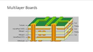
Short Overview: Multidisciplinary product creation powered by your unconstrained network. This video looks at how changing the order and function of layers can have significant impacts on performance.

Pcb Stackup Design Process Thought Process Explained - Starter Guide

Use this page to review Pcb Stackup Design Process Thought Process Explained with quick summaries, related pages, and practical search paths with enough structure to compare related entries.

In addition, this page also connects Pcb Stackup Design Process Thought Process Explained with for broader topic coverage.

Starter Guide

Multidisciplinary product creation powered by your unconstrained network. This video looks at how changing the order and function of layers can have significant impacts on performance.

Common Details

This section highlights the practical pieces readers may want before opening a more specific related page.

Reference Comparison Context

Context matters because Pcb Stackup Design Process Thought Process Explained can connect to nearby topics, related searches, and different reader intents.

Reference Follow-Up Tips

Use the related entries as follow-up paths when you need more examples, current details, or alternative wording.

Relevant points collected here

  • This video looks at how changing the order and function of layers can have significant impacts on performance.
  • Multidisciplinary product creation powered by your unconstrained network.

Why this topic is useful

A structured page helps by giving readers a simple summary for Pcb Stackup Design Process Thought Process Explained so they can continue with better search intent.

Sponsored

Questions People Also Check

How can readers make Pcb Stackup Design Process Thought Process Explained more specific?

Different pages may focus on different locations, dates, providers, versions, definitions, or user needs.

Why do people search for Pcb Stackup Design Process Thought Process Explained?

People often search for Pcb Stackup Design Process Thought Process Explained to understand the basics, compare related options, or find a clearer path to more specific information.

Is this page a final source?

No. It is best used as a quick reference and discovery page before checking stronger or official sources.

What is the safest way to use Pcb Stackup Design Process Thought Process Explained information?

Use it as general context first, then verify important points with official, primary, or more specific sources when accuracy matters.

Related Media Gallery

PCB Stackup Design Process Thought Process Explained!
The Fundamentals of PCB Stackup Design
PCB stackup impact on performance
Introduction to Basic Concepts in PCB Design
PCB Stack-Up and Build-Up - Phil's Lab #56
ALL OF PCB Design Explained Simply
Signal Ground Power Ground 4-Layer Stackup? PCB Design Explained!
Understanding 2+n+2 Stackups in HDI Design
Secrets of PCB Optimization - Rick Hartley - AltiumLive 2020
How to Decide on Your PCB Layer Ordering, Pouring and Stackup (with Rick Hartley)
Sponsored
Read the Full Notes
PCB Stackup Design Process Thought Process Explained!

PCB Stackup Design Process Thought Process Explained!

Read more details and related context about PCB Stackup Design Process Thought Process Explained!.

The Fundamentals of PCB Stackup Design

The Fundamentals of PCB Stackup Design

Read more details and related context about The Fundamentals of PCB Stackup Design.

PCB stackup impact on performance

PCB stackup impact on performance

This video looks at how changing the order and function of layers can have significant impacts on performance. This video also ...

Introduction to Basic Concepts in PCB Design

Introduction to Basic Concepts in PCB Design

Read more details and related context about Introduction to Basic Concepts in PCB Design.

PCB Stack-Up and Build-Up - Phil's Lab #56

PCB Stack-Up and Build-Up - Phil's Lab #56

Read more details and related context about PCB Stack-Up and Build-Up - Phil's Lab #56.

ALL OF PCB Design Explained Simply

ALL OF PCB Design Explained Simply

Read more details and related context about ALL OF PCB Design Explained Simply.

Signal Ground Power Ground 4-Layer Stackup? PCB Design Explained!

Signal Ground Power Ground 4-Layer Stackup? PCB Design Explained!

Multidisciplinary product creation powered by your unconstrained network. Work concurrently across

Understanding 2+n+2 Stackups in HDI Design

Understanding 2+n+2 Stackups in HDI Design

Read more details and related context about Understanding 2+n+2 Stackups in HDI Design.

Secrets of PCB Optimization - Rick Hartley - AltiumLive 2020

Secrets of PCB Optimization - Rick Hartley - AltiumLive 2020

Multidisciplinary product creation powered by your unconstrained network. Work concurrently across

How to Decide on Your PCB Layer Ordering, Pouring and Stackup (with Rick Hartley)

How to Decide on Your PCB Layer Ordering, Pouring and Stackup (with Rick Hartley)

Do you pour copper on your signal layers or not? Thank you very much Rick Hartley. Credits to Daniel Beeker, Lee Ritchy and ...